Scanning Electron Microscopy (SEM) is one of the most powerful tools for studying surface morphology at micro-scale resolution. It reveals particle size, surface texture, micro-cracks, coating quality, and structural features that are invisible to optical microscopes. However, high-quality SEM results depend heavily on proper sample preparation.
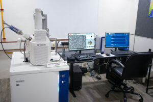
At the Micro–Nano Research & Development Center (MNRDC), SEM analysis is carried out using a state-of-the-art system integrated with Energy Dispersive Spectroscopy (EDS) for elemental verification. Since SEM operates under vacuum and uses a focused electron beam, strict preparation protocols must be followed to prevent contamination, inaccurate imaging, or equipment damage.
This guide explains SEM sample preparation in four critical stages: drying, coating, mounting, and rejection criteria.
Why Sample Preparation Is Critical in SEM
SEM works by generating an electron beam from a tungsten filament and focusing it onto the sample using condenser and objective lenses. The instrument requires approximately five minutes to create a vacuum before operation.
Because imaging occurs inside a sealed vacuum chamber, any moisture, loose particles, or unstable material can:
- Contaminate the chamber
- Distort imaging
- Damage sensitive components
- Produce charging effects
Proper preparation ensures clear imaging at common resolution ranges such as 30 µm, 10 µm, and 5 µm.
Drying: The First and Most Important Step
Accepted Sample Types
SEM can analyse:
- Solid samples
- Liquid samples (only after drying)
- Semi-solid samples (only after drying)
However, only dried samples are allowed inside the SEM chamber.
Drying Procedure
Liquid and semi-solid samples are dried at approximately 30–40°C using controlled heating in the preparation room.
Drying ensures:
- No vapour formation under vacuum
- No bubbling or sample expansion
- No contamination inside the chamber
What Gets Rejected During Drying
Samples will be rejected if:
- They contain residual moisture
- They release vapours under vacuum
- They deform excessively during drying
- They remain sticky or unstable after drying
Moisture contamination is the most common cause of SEM rejection.
Coating: Making Samples Conductive
SEM imaging requires electrical conductivity. Non-conductive samples accumulate charge under the electron beam, causing image distortion.
Gold Coating
Non-conducting samples undergo gold coating to make them conductive. The coating thickness is customizable depending on sample requirements.
Gold coating:
- Prevents surface charging
- Improves image clarity
- Enhances resolution
- Produces sharper morphological details
Conductive materials (like metals) typically do not require coating.
What Gets Rejected During Coating
Samples may be rejected if:
- Surface is contaminated with oil or dust
- The material is too soft and gets damaged during coating
- Sample reacts chemically to coating conditions
- Sample geometry prevents uniform coating
Improper coating can result in uneven brightness, streaking, or imaging artefacts.
Mounting: Secure and Stable Placement
Correct mounting ensures that the sample remains stable during stage movement and imaging.
Mounting Materials
- Carbon tape is used for solid samples.
- Copper tape is used for dried liquid and semi-solid samples.
Mounting Discs
Commonly used mounting discs include:
- 50 mm
- 125 mm.
The sample is fixed onto the disc and then placed on the SEM stage. Proper centre placement ensures:
- Accurate focus
- Clear imaging
- Correct working distance
The stage moves upward to position the sample inside the chamber. After closure, automatic adjustments align the sample for imaging.
Chamber Safety Rule
The chamber must remain closed except during sample insertion or stage motion to prevent atmospheric contamination.
What Gets Rejected During Mounting
A sample will be rejected if:
- It does not fit on the standard disc
- It is loosely attached
- Powder particles are unstable
- It exceeds height limits
- It interferes with stage movement
Improper mounting can cause vibration, misalignment, or damage to the detector.
Instrument Settings and Power Considerations
Correct voltage selection is essential to prevent sample damage.
Power ranges:
- Solids: 5–30 kV
- Liquids/Semi-solids: 3–15 kV.
Higher voltage improves resolution, but excessive voltage can damage delicate or sensitive samples.
An incorrect material declaration may lead to inappropriate voltage selection and potential sample rejection.
Final Output and Handling
Each sample typically generates:
- 8 SEM images from multiple magnifications
- 2 EDS spectra (if requested).
Standard SEM analysis takes approximately 45 minutes, while SEM + EDS requires around 60 minutes.
Proper preparation ensures that this time produces reliable, high-quality data.
Common Rejection Criteria Summary
A sample will likely be rejected if it is:
- Wet or improperly dried
- Highly volatile under vacuum
- Poorly mounted or unstable
- Too large for standard discs
- Contaminated with dust or oil
- Extremely beam-sensitive
- Loose powder without proper fixing
- Causing repeated charging even after coating
These rules protect both the equipment and the integrity of analytical results.
Conclusion
SEM is a precision instrument designed to reveal microscopic details with remarkable clarity. However, the accuracy of results depends entirely on correct sample preparation.
Proper drying prevents vacuum contamination. Gold coating ensures conductivity. Secure mounting guarantees stability. Understanding rejection criteria prevents delays and protects equipment.
At MNRDC, SEM preparation is not just a procedural step; it is the foundation of reliable micro-scale imaging and elemental analysis.