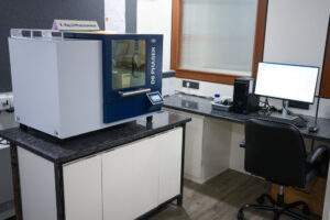
How AFM Works: The Basic Principle
p class=”mt-3″>At the heart of AFM is a tiny, ultra-sharp tip (radius ~5–10 nm) mounted on a flexible cantilever. Imagine a miniature diving board with a needle at its end.
AFM operates using Hooke’s Law (F = –kx) :
- F = force
- k = spring constant of the cantilever
- x = deflection distance
As the tip scans across the surface:
- It encounters microscopic hills and valleys.
- The cantilever bends upward or downward.
- A laser beam reflected from the cantilever detects this bending.
- A photodetector records the change and converts it into height data.
The result is a highly detailed 2D and 3D map of the surface.
AFM works primarily through Van der Waals forces, the invisible atomic forces that occur when atoms get very close to each other.
Types of AFM Imaging Modes
AFM has several modes that control how the tip interacts with the surface. Each mode is suited to different materials and applications.
(a) Contact Mode
In Contact Mode, the tip physically drags across the surface like a record player needle.
Advantages:
- Very high resolution
- Simple operation
Limitations:
- Can scratch soft materials
- May wear out the tip faster
- Not ideal for delicate samples like biological tissues
Contact mode is suitable for hard, durable materials such as metals and certain ceramics.
(b) Non-Contact Mode
In Non-Contact Mode, the tip hovers just above the surface without physically touching it.
Instead of contact, it senses the attractive atomic forces between the tip and the sample.
Advantages:
- No surface damage
- Long tip life
- Suitable for soft or sensitive materials
Limitations:
- Slightly lower resolution compared to contact mode
- Sensitive to environmental noise
Non-contact mode is ideal for delicate biological samples or soft polymers.
(c) Tapping Mode (Dynamic Mode)
Tapping Mode is the most commonly used mode. Here, the tip vibrates up and down at high frequency, gently “tapping” the surface hundreds of thousands of times per second.
Advantages:
- Gentle on soft materials
- High resolution
- Reduced lateral damage
- Excellent balance between safety and accuracy
Because it minimises surface damage while maintaining image clarity, tapping mode is widely used for studying nano-coatings, semiconductor layers, and optical components.
What Does AFM Output Look Like?
AFM produces three primary types of output:
- 2D Image
A flat, top-down map where colour represents height (dark = valleys, bright = peaks).
- 3D Image
A mountain-like surface visualisation that makes nanoscale terrain appear realistic.
- Topography Data
Precise numerical height data used for measurements.
During scanning, the tip typically covers an area such as 10 × 10 µm, moving line-by-line (for example, 256 scan lines) to generate detailed maps.
What Do Roughness Reports Mean?
One of the most requested outputs from AFM analysis is the surface roughness report.
Roughness values are numerical indicators of how smooth or uneven a surface is. These reports are generated using specialised analysis software that can calculate over 50 ISO-standard roughness parameters.
Common Roughness Indicators:
- Average Roughness (Ra): The average height variation from the mean surface line.
- Root Mean Square Roughness (Rq): A more sensitive measurement of surface variation.
- Peak-to-Valley Height: The difference between the highest peak and the deepest valley.
Why Roughness Matters
Surface roughness directly impacts performance:
- Optical lenses: Roughness must be below certain limits (e.g., below 100 nm) to prevent irritation or distortion.
- Semiconductors: Excess roughness may cause electronic failure.
- Coatings: Smooth surfaces improve adhesion and durability.
- Biomedical implants: Surface texture affects tissue compatibility.
AFM also generates histograms and grain analysis graphs, which show particle size distribution across the scanned area.
Beyond Imaging: Advanced AFM Capabilities
AFM is not limited to surface mapping. Depending on the mode, it can measure:
- Adhesion and stiffness (force spectroscopy)
- Magnetic properties (MFM mode)
- Electrical charge distribution (EFM mode)
- Nano-indentation and mechanical response
AFM can also operate in air, liquid, or vacuum environments, making it versatile for various sample types.
Why AFM Is So Powerful
The biggest strength of AFM is precision. It does not estimate or approximate surface structure; it physically measures atomic-scale forces.
While XRD reveals internal atomic structure and SEM shows surface morphology, AFM measures actual surface smoothness at nanometer resolution.
It provides both visual and quantitative confirmation of material quality.
Conclusion
Atomic Force Microscopy is like having a nano-scale fingertip combined with ultra-precise measurement software. Whether operating in contact, non-contact, or tapping mode, AFM converts atomic forces into measurable surface maps.
Understanding roughness reports helps engineers determine whether a surface is smooth enough, strong enough, or uniform enough for real-world applications.
In modern materials science, surface quality defines performance, and AFM makes that invisible world measurable, one nanometer at a time.