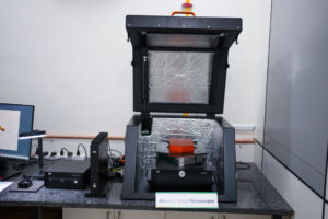
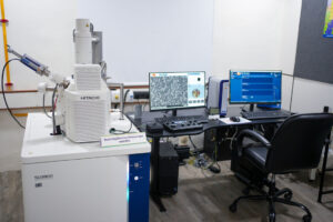
X-Ray Diffraction (XRD) is one of the most powerful techniques used to understand what a material is made of at the atomic level. While microscopes like SEM show the surface “face” of a material, XRD looks at its internal atomic “skeleton”. It helps scientists determine crystal structure, phase composition, stress, and even crystal size, all without damaging the sample.
This article explains XRD in a simple way, focusing on Bragg’s Law, diffraction peaks, and how materials are identified.
What Does XRD Actually Do?
XRD allows us to look inside a solid and determine:
- Atomic structure
- Chemical composition
- Physical properties
It works especially well for crystalline materials, substances where atoms are arranged in a repeating, orderly pattern (like a carton of eggs stacked neatly).
Unlike surface imaging tools, XRD uses X-rays because their wavelength (~0.1 nm) is almost the same size as the spacing between atoms in crystals. This makes X-rays the perfect “ruler” for measuring atomic spacing.
XRD can analyse powders, bulk solids, and thin films.
The Heart of XRD: Bragg’s Law
At the core of XRD lies a simple but powerful equation known as Bragg’s Law:
nλ = 2d sinθ
Where:
- λ (lambda) = wavelength of the X-ray
- θ (theta) = angle at which X-rays hit the crystal
- d = spacing between atomic layers
- n = order of reflection (usually 1)
What Does This Mean?
When X-rays hit a crystal, atoms scatter the rays in different directions. Most scattered waves cancel each other out. But at specific angles, the waves line up perfectly and reinforce each other. This is called constructive interference.
Bragg’s Law tells us exactly when this “perfect alignment” happens. When the condition is satisfied, a strong signal is detected. These strong signals appear as peaks on an XRD graph.
In simple words:
Bragg’s Law translates the bounce of X-rays into a map of atomic spacing.
Understanding the XRD Graph
The output of an XRD test is a graph with:
- X-axis: 2θ (angle)
- Y-axis: Intensity (strength of reflected X-rays)
This graph acts like a barcode or fingerprint of the material.
What Are the Peaks?
The sharp spikes or “mountains” on the graph are called diffraction peaks.
Each peak appears when X-rays hit perfectly aligned atomic layers.
The position of the peak tells us:
- What the material is
- How atoms are arranged
The height of the peak tells us:
- How much of that phase is present
The width of the peak tells us:
- Whether crystals are large (sharp peaks) or nano-sized (broader peaks)
Crystalline vs Amorphous Materials
Crystalline materials: Show sharp, tall peaks because atoms are well-organised.
Amorphous materials (like glass): Show a wide hump instead of sharp peaks because atoms are randomly arranged.
How Material Identification Works
Every crystalline material has a unique atomic arrangement. That arrangement produces a unique diffraction pattern.
Think of it like fingerprints. No two materials have exactly the same peak positions.
To identify a material:
- The XRD scan produces a diffraction pattern.
- The peak positions (2θ values) are compared with reference data.
- If the peaks match a known pattern, the material is identified.
The system uses the ICDD database, which contains over one million reference patterns. Each reference file (PDF – Powder Diffraction File) lists where peaks should appear for a known material.
If your sample’s peaks match a reference PDF, the identity is confirmed.
Advanced Analysis: Quantification & Refinement
Modern XRD doesn’t stop at identification. It can also determine:
- Percentage of each phase in a mixture
- Stress in crystals
- Exact lattice parameters
Using advanced software like TOPAS, the system applies the Rietveld Method.
Here’s how it works:
- You propose what materials may be present.
- The software calculates a theoretical diffraction pattern.
- It compares the calculated pattern with the real measured graph.
- It adjusts atomic positions and crystal parameters until both match perfectly.
The result is a highly accurate, quantitative breakdown of material composition.
Special Modes for Thin Films
For very thin coatings, standard XRD may detect mostly the base material. To solve this:
- GIXRD (Grazing Incidence XRD) uses a very small incident angle (less than 1°) to focus only on the surface layer.
- XRR (X-Ray Reflectivity) measures coating thickness (1–500 nm), roughness, and density.
These techniques are especially useful for nano-coatings and semiconductor layers.
Why XRD Is So Powerful
One of the biggest advantages of XRD is that it is a Non-Destructive Testing (NDT).
- The sample is not burned or melted.
- No chemical coating is required.
- The material remains intact and reusable.
This makes XRD ideal for valuable samples like advanced composites, rare minerals, or high-cost engineered materials.
Real-World Applications
XRD is widely used in:
- Pharmaceuticals (drug phase identification)
- Construction (cement analysis)
- Electronics (thin-film verification)
- Battery research (phase monitoring)
- Aerospace (stress analysis)
It helps engineers optimise processes; for example, checking if heat treatment successfully changed a metal phase from softer Austenite to harder Martensite.
Conclusion
XRD may look complex at first, but its foundation is simple: X-rays bounce off atomic layers, and at special angles defined by Bragg’s Law, they create peaks. These peaks form a unique fingerprint of the material.
By analysing peak positions, heights, and widths, and comparing them with reference databases, scientists can confidently identify materials and quantify their composition.
For students, understanding Bragg’s Law and diffraction peaks unlocks the gateway to atomic-scale material science. XRD turns invisible atomic arrangements into readable, scientific barcodes, revealing exactly what a material is and how it is built.